




Verified recordCommercial · Texas InstrumentsUpdated 2026-10-01
TPS5430DDAR
Manufactured by Texas Instruments. Verified supply on file.
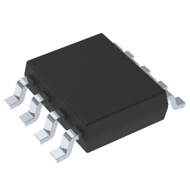
Specifications
FunctionStep-Down
Output ConfigurationPositive
TopologyBuck
Output TypeAdjustable
Number of Outputs1
Voltage - Input (Min)5.5V
Voltage - Input (Max)36V
Voltage - Output (Min/Fixed)1.221V
Voltage - Output (Max)32.04V
Current - Output3A
Datasheet
Source: Texas InstrumentsView on manufacturer site ↗
Overview
The TPS5430DDAR is a 3A, step-down (buck) regulator with an integrated high-side n-channel MOSFET. It is a high-output-current PWM converter that implements constant-frequency voltage-mode control with voltage feed forward for improved line regulation and line transient response. Internal compensation reduces design complexity and external component count. The integrated 100mΩ high-side MOSFET supports high-efficiency power-supply designs capable of delivering 3A of continuous current to a load. The TPS5430 regulates a wide variety of power sources including 24V bus.
Key features
- Wide input voltage range: 5.5V to 36V (for TPS5430)
- Up to 3A continuous (4A peak) output current
- High efficiency up to 95% enabled by 100mΩ integrated MOSFET switch
- Wide output voltage range: adjustable down to 1.22V with 1.5% initial accuracy
- Internal compensation minimizes external parts count
- Fixed 500kHz switching frequency for small filter size
- Improved line regulation and transient response by input voltage feedforward
- System protected by overcurrent limiting, overvoltage protection, and thermal shutdown
- –40°C to 125°C operating junction temperature range
- Available in small thermally enhanced 8-pin SO PowerPAD™ integrated circuit package
Pinout / functions
BOOT (1)Boost capacitor for the high-side FET gate driver. Connect 0.01μF low ESR capacitor from BOOT pin to PH pin.
NC (2)Not connected internally.
NC (3)Not connected internally.
VSENSE (4)Feedback voltage for the regulator. Connect to output voltage divider.
ENA (5)On and off control. Below 0.5V, the device stops switching. Above 1.3V, the device starts switching. ENA can be left floating. This pin is internally connected to a 1.5MΩ pullup resistor. Do not connect this pin with a resistor to ground.
GND (6)Ground. Connect to DAP.
VIN (7)Input supply voltage. Bypass VIN pin to GND pin close to device package with a high quality, low ESR ceramic capacitor. Place the bypass capacitor within 1mm of the Vin pin and within 1mm of the GND pin.
PH (8)Source of the high side power MOSFET. Connected to external inductor and diode.
DAPGND pin must be connected to the exposed pad for proper operation.
Applications
Applications for this part include consumer electronics such as set-top boxes, DVD players, and LCD displays, as well as industrial and car audio power supplies. It can also be used in battery chargers, high-power LED supplies, and 12V and 24V distributed power systems.
Alternates / same series
TPS5430Input voltage range 5.5V to 36V
TPS5431Input voltage range 5.5V to 23V
FAQ
What is the input voltage range for the TPS5430?
The TPS5430 has an input voltage range of 5.5V to 36V.
What is the continuous output current capability?
The device can provide up to 3A continuous output current, with a 4A peak.
What is the switching frequency of the TPS5430?
The TPS5430 has a fixed 500kHz switching frequency.
What is the operating junction temperature range?
The operating junction temperature range is –40°C to 125°C.
What package is the TPS5430DDAR available in?
The TPS5430DDAR is available in a thermally enhanced 8-pin SO PowerPAD™ integrated circuit package (DDA HSOIC, 8).
Availability
SupplyVerified supply chain on file
Lead timeQuoted on request
TraceabilityFull documentation with every shipment
BTEK sources through registry-verified producers, authorized distributors and vetted independent channels. Certs of conformance travel with the parts.
Market price estimate: from $2.82 ea @ 100 pcs
Final price depends on quantity, lead time, date code range, CofC / certs and third-party inspection. Not an offer.
Captured 2026-10-05
Get a quote in minutes.
Quantity and target date. BTEK's quoting engine sources, prices and replies by email.
BTEK Components MFG LLC · Largo, FloridaPart data compiled and verified by BTEK's sourcing engine.